


Why Choose Consons EMI PCB Board?
- Continuous Ground Plane Design: Provides uninterrupted reference planes to reduce return loop areas, effectively trapping electromagnetic radiation within the board. This reduces stray noise, prevents crosstalk, and improves signal stability for complex circuits.
- DFM EMI Pre-Screening: Our expert DFM review identifies potential EMI risks before production starts. This reduces costly re-spins, minimizes upfront development expenses, and significantly increases your first-pass yield rate.
- Made with High-Frequency Materials: Standard FR-4 laminates exhibit high dielectric loss at high frequencies. Consons selects high-frequency materials with low Dk and low Df, like Rogers or high-TG FR-4, for EMI PCB laminates to improve transmission stability.
- Compact EMI PCB Design for Limited Space: Integrates embedded shielding, via fences, and optimized micro-stackups into ultra-compact layouts. Get excellent electromagnetic isolation and good signal integrity without increasing board size, perfect for high-density electronic products.
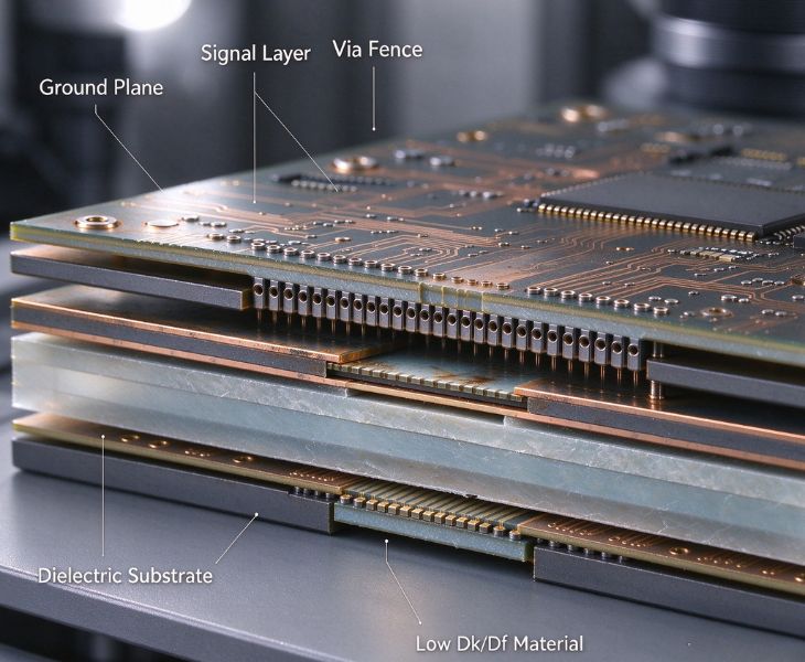
What Is EMI and EMC in PCB?
Electromagnetic interference (EMI) refers to unwanted electromagnetic energy generated by electronic devices or introduced into electronic circuits. Electromagnetic compatibility (EMC) covers a wider scope and aims to ensure devices operate properly in their intended electromagnetic environment without causing interference to other devices.
Almost all common electronic products must meet EMC requirements. Otherwise, they cannot enter the market. With 20 years of experience in PCB R&D and manufacturing, Consons offers flexible EMC PCB solutions across a variety of materials, structures, and functional requirements. These solutions are designed to help you adapt flexibly to a wide range of applications.
Send Consons your BOM and Gerber files. We will conduct a comprehensive evaluation of your EMI PCB and provide you with a competitive quote.
EMI PCB Provided by Consons
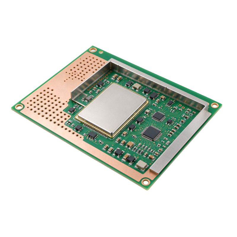
Ground planes, via stitching, and shielding structures reduce electromagnetic radiation and coupling. Improves noise isolation for RF modules, wireless devices, automotive electronics, and high-speed circuits.

Integrates embedded capacitors and common-mode chokes to reduce power-line noise. Prevents conducted emissions, delivering clean voltage to noisy industrial and automotive electronics.
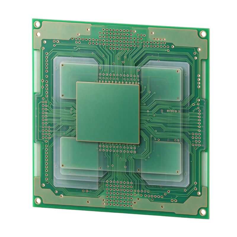
Multi-layer stackups with continuous ground planes shrink return loops. Suitable for complex high-speed electronics, networking equipment, automotive controllers, and industrial systems.
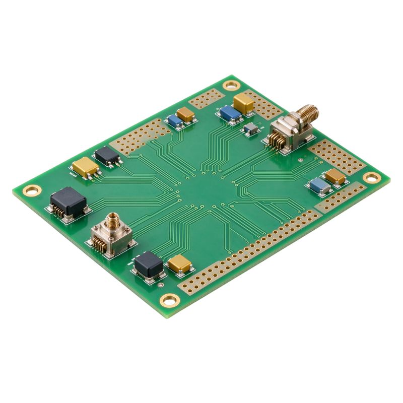
Crafted with low-loss materials and tight impedance control. Reduces signal jitter and crosstalk, enabling flawless high-speed transmission in radar and satellite communications.
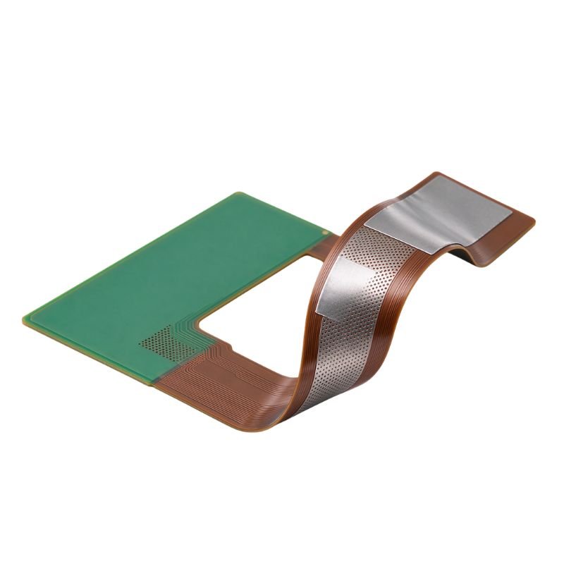
Combines flexible substrates with a shielding layer. Prevents noise leaks at dynamic bends, making it ideal for compact wearables and foldables.
Guaranteed PCB EMC Compliance
Consons’ advanced EMI PCB fabrication helps eliminate product launch delays and costly redesigns. We engineer layer stackups and ground plane continuity directly aligned with international standards, including FCC, CE, CISPR 25, and IEC 60601. By reducing high-frequency noise and radiative emissions during the pre-manufacturing DFM stage, we drastically reduce unwanted electromagnetic coupling. Consons can help your complex electronic assemblies pass strict EMC testing more easily. This protects your significant project times, budget, and market entry schedules seamlessly.

Precision Impedance and Signal Integrity Control
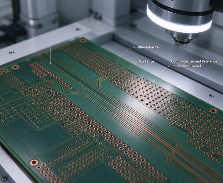
Consons’ precise PCB manufacturing processes maximize circuit performance and prevent high-speed data distortion. We deliver tight impedance tolerances within ±5%, using premium low-loss materials, specialized via fencing, and continuous reference planes to eliminate signal reflections, jitter, and crosstalk. Our strict trace geometry controls keep return paths short and electromagnetic noise trapped within the board structure. This makes our EMI PCBs perfect for DDR, PCIe, and 5G RF applications. Consons will offer your products flawlessly clear data transmission and stable operational performance under demanding high-frequency operating conditions.
Why Is Consons Your Reliable Partner?

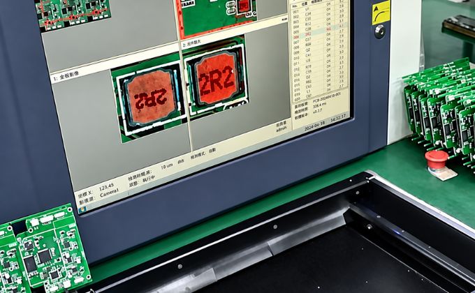
Consons offers a true turnkey service, including prototyping, procurement, PCB manufacturing, PCB assembly, and a full range of other services. You won’t need to coordinate with multiple factories, saving you significant time and effort. Our client base includes leading brands across multiple sectors like consumer electronics, automotive, industrial control, and smart home, including Samsung, Mercedes-Benz, Siemens, and more.
Consons’ headquarters facility spans 35,000 square meters and features separate production zones. With a team of 1,600 highly skilled employees, we have a monthly production capacity of 100,000 square meters for rigid PCBs and 50,000 square meters for flexible PCBs. You can confidently entrust us with your high-volume orders. We guarantee on-time delivery.
EMI PCB Specifications
| Parameter | EMI PCB Specification |
| PCB Type | Rigid PCB, Multilayer PCB, High-Frequency PCB, Impedance-Controlled PCB, Flex / Rigid-Flex PCB |
| Layer Count | 1–30 Layers |
| Base Materials | FR-4, High-Tg FR-4, Rogers, Taconic, Argon, and other application-specific laminates |
| High-Frequency Materials | Rogers / Taconic and other low-loss materials available for RF and high-speed applications |
| Copper Thickness | Standard Copper: 0.5–3 oz; Heavy Copper: Up to 60 oz |
| Minimum Line Width / Spacing | 3.5 / 4 mil |
| Minimum Mechanical Drill | 0.15 mm |
| Minimum Laser Drill | 4 mil |
| Minimum Annular Ring | 4 mil |
| Maximum Board Size | 900 × 1200 mm |
| Standard Board Thickness | 0.2–7.0 mm |
| Solder Mask Bridge | Min. 0.18 mm |
| Impedance Control | Controlled-impedance PCB fabrication for high-speed and RF signal transmission |
| EMI Control Structures | Ground planes, controlled return paths, via stitching / via fencing, shielding structures according to design requirements |
| Surface Finish | HASL, Lead-Free HASL, ENIG, OSP, Immersion Silver, Flash Gold, Gold Finger, Immersion Tin |
| Solder Mask Colors | Green, Red, Yellow, White, Blue, Black |
| Via Plugging | 0.2–0.8 mm plugging via capability |
| Plated Hole Tolerance | ±0.05 mm minimum, according to design requirements |
| Non-Plated Hole Tolerance | ±0.05 mm minimum, according to design requirements |
| Outline Tolerance | ±0.10 mm minimum |
| Functional Electrical Test | Electrical continuity and insulation testing available |
| Insulation Resistance | ≥10⁸ Ω |
| Peel Strength | ≥1.4 N/mm |
| Thermal Stress Test | 288°C, 10 seconds, 3 cycles |
| E-Test Voltage | 500 V ±15 V, 30 seconds |
| Warp & Twist | ≤0.7%; semiconductor test boards ≤0.3% |
| Aspect Ratio | 10:1 |
Project Case of Consons EMI PCB

The client’s high-speed medical monitor failed CISPR 11 EMC testing due to strong clock noise. Standard FR-4 boards caused severe signal crosstalk and delayed market entry.
Consons ran a PCB EMI simulation to map near-field noise and pinpoint radiating loops before fabrication. We replaced FR-4 with high-frequency Rogers laminates and used a 6-layer sandwich stackup with continuous ground planes. We also added a via fence around high-speed traces and pre-installed SMT shielding pads. This eliminated crosstalk, reduced radiation by 18 dB, and helped the client pass European medical certification on the first try.

The client faced high-frequency power noise on DC-DC lines. Switching noise interfered with nearby radio units, while tight enclosure space prevented using large external metal shields.
Consons selected an embedded EMI filtering PCB solution. We integrated low-ESR decoupling capacitors directly into the inner layer stackup right beneath the power ICs. We also applied a customized conductive silver paste printing on the board surface. This compact design suppressed conducted emissions by 25 dB without expanding the PCB footprint, offering reliable performance under hot outdoor conditions.
You Can Use Our EMI PCB for:

EMI PCBs help control interference in EV battery management systems, onboard chargers, vehicle displays, ADAS controllers, and LED lighting. They support reliable communication, stable sensing, and consistent operation in electrically noisy environments.

EMI PCBs can limit electromagnetic coupling and signal interference to preserve high-speed data transmission, wireless performance, and stable communication between densely packed circuits. They are a good choice for smartphones, Wi-Fi routers, 5G modules, RF transceivers, and network switches.
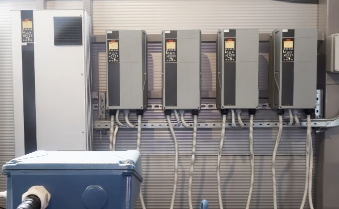
EMI PCBs reduce switching noise and protect sensitive control signals from interference generated by high-current power circuits. Widely used in PLCs, motor drives, inverters, switching power supplies, industrial sensors, and machine status indicators.

EMI PCBs are suitable for medical monitors, smart speakers, household lighting, LED indicators, smart appliances, and wearable devices. These compact layouts and sensitive electronic circuits demand lower electromagnetic noise without compromising reliable operation.
More Products
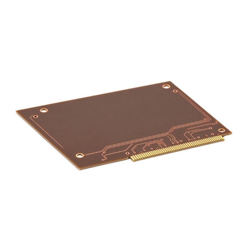
Low-loss Rogers laminates maintain stable dielectric performance and controlled impedance, reducing high-frequency signal loss for RF modules, antennas, radar systems, 5G communication equipment, and high-speed circuits.
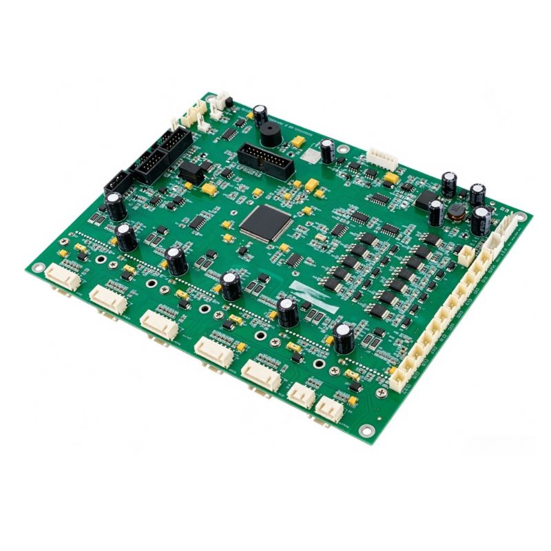
Halogen-free flame-retardant materials support reliable insulation and environmental compliance. Suitable for consumer electronics, automotive systems, industrial controls, and environmentally conscious products.
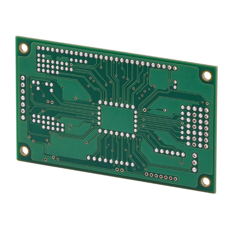
Aluminum or copper cores efficiently transfer heat away from power components, improving thermal management for LED lighting, power supplies, motor controllers, automotive electronics, and high-current circuits.

Common EMI shielding materials used in PCBs primarily include copper foil, board-level shielding cans, high-frequency laminates, and absorbing sheets. In board-level design, nickel silver or tin-plated steel shielding cans can directly shield RF modules. High-frequency laminates, like Rogers or high-Tg FR-4, can reduce dielectric loss at the source. Conductive silver ink and electromagnetic shielding films are the top choice for achieving lightweight, thin radiation shielding for flexible PCBs.
The main difference between the two is the transmission medium. Radiated EMI refers to high-frequency electromagnetic waves that propagate directly through space or air and interfere with external circuits. It is commonly found in high-frequency clock and antenna wiring. Conducted EMI refers to noise that is transmitted directly along physical conductors (including power lines, signal traces, or cables). In one sentence, radiated interference is noise that propagates wirelessly, while conducted interference is noise that is transmitted through wired traces. In testing, these correspond to RE and CE evaluations.
The key to controlling conducted noise is blocking the propagation of interference along the power and signal paths. During PCB manufacturing and design, we optimize the layer stackup and use a continuous ground plane to provide a low-impedance return path. At the same time, we place decoupling capacitors in a compact layout adjacent to power pins and embed common-mode chokes and LC filter networks at the interfaces. Combined with a well-designed power plane split, this effectively confines high-frequency conducted ripple to a limited area, preventing it from leaking into external cables.
Many common factors cause EMI test failures. For example, a discontinuous ground plane can result in an excessively large signal return loop area. High-speed signal lines routed across partition lines. Failure to perform precise impedance control leads to signal reflections. The absence of a via fence around the edges of high-frequency traces leads to radiated leakage. Additionally, power decoupling capacitors placed too far from the chip pins cannot effectively filter the signal. These potential issues can all be promptly corrected through Consons’ DFM review.
Evaluating the EMI performance of a PCB typically involves near-field diagnostics and standard certification testing. During the R&D and prototyping stages, near-field probes and spectrum analyzers are primarily used to quickly locate radiation hotspots on the board. During the compliance certification phase, conducted emission (CE) and radiated emission (RE) tests must be conducted in an anechoic chamber, while evaluating immunity (EMS), to ensure that the board complies with international industry standards such as FCC, CE, or CISPR 25.
Absolutely. Consons has 15 fully automated SMT production lines that support high-precision automated assembly of SMT shield cans and conductive gaskets. We recommend that customers use tape-and-reel packaging to enable high-speed pick-and-place operations on the SMT machines. Additionally, we precisely control the temperature zones during the reflow soldering to ensure that the shield frames are securely soldered without any cold solder joints, significantly improving both the lead time and yield rate of our one-stop turnkey SMT assembly services.
For flex PCBs and rigid-flex PCBs, Consons offers various highly bend-resistant surface shielding solutions. Including conductive silver ink, laminated composite shielding films such as Tatsuta films, and cross-hatch copper shielding designs. These solutions provide up to 30–50 dB of radiated shielding effectiveness for high-speed signals without compromising the flexing and bending durability of the PCB, making them a good choice for foldable devices and camera modules.