


One-Stop AI PCB Manufacturing & Assembly Services for Next-Gen Communications
CONSONS AI PCB is specially built for next-generation communication equipment. Compared with ordinary PCBs, it meets higher requirements in high-speed signal transmission, high-density interconnection, low signal loss, etc. We design and manufacture multi-layer AI PCBs with up to 40+ layers, single-channel 112G transmission rates, and ±5% impedance tolerances, providing a stable high-speed data transfer foundation.
From PCB manufacturing and PCBA assembly to FPC manufacturing, component supply chain management, injection molding, automated assembly, testing, and finished product packaging, we provide a complete AI PCB manufacturing and assembly process. Through AOI and X-Ray inspection, we identify soldering defects and hidden solder joint problems, while the engineering team provides DFM review and production optimization support. The one-stop model shortens the move from samples to batch production.
Get an AI PCB quote today and choose a one-stop manufacturing solution for your next generation communications project.
AI PCB Types

The multilayer structure handles complex routing and power distribution across dense backplanes in AI servers with multiple conductive layers to improve the high-speed signal integrity of compact communication hardware.

The microvias, blind vias, and their sequential buildup structures improve routing density while reducing board size, making them suitable for demanding electronics like 5G radios or optical transceiver modules

The rigid and flexible sections are combined to reduce connectors and simplify interconnections, and improve reliability in foldable or vibration conditions for space-constrained electronic systems.

It supports compact layouts, complex interconnections, for high-power AI hardware with ultra-fine pitch, high I/O count, as well as optimized routing.

It is produced with precise fine-line and fine-space, supporting dense routing, fine-pitch components, and precise impedance control, which is important for 224G high-speed serial links and loss-sensitive channels.

The M8/M9 ultra low loss materials with Df < 0.0015 reduce dielectric attenuation in 112G/224G PAM4 high-speed digital links that have requirements for high-speed and long-reach transmission.
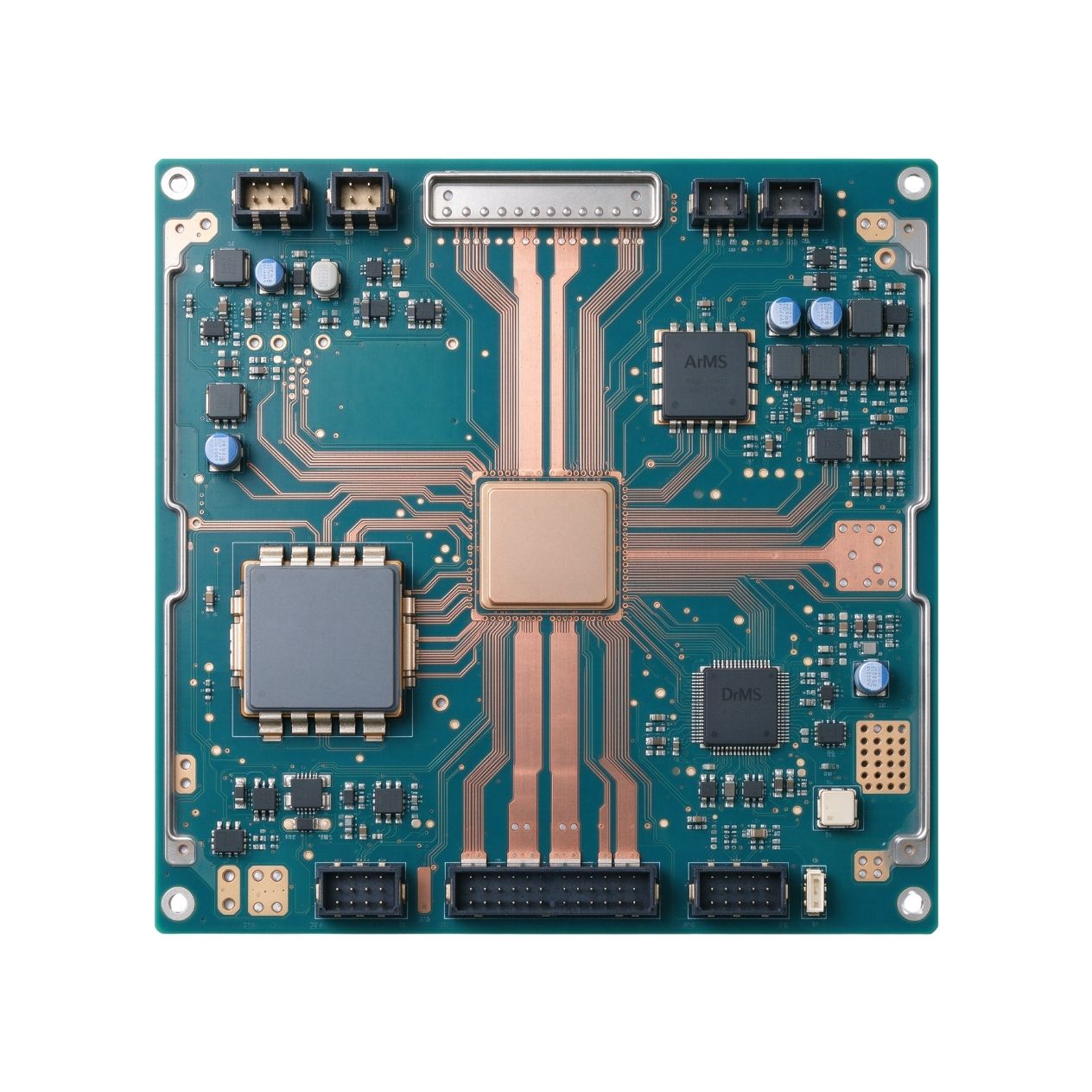
By optimizing copper structures, power distribution, and heat dissipation designs, it can handle >100A currents and thermal loads for power-intensive systems.
Extreme Thermal Management
Our thermal management solutions combine MCPCB technology, heavy copper layers, embedded copper coins, and high thermal conductivity dielectric materials to establish an efficient heat dissipation path inside the AI PCB structure, quickly dissipate heat away from key components, reduce heat accumulation, and help the device maintain stability at continuous high-power operation. The thermal design can be customized based on component power, temperature limits, and system cooling conditions, avoiding frequency reduction and greatly extending the service life of your equipment.

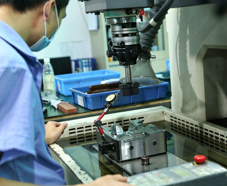
Precision Enclosure
Our AI PCB manufacturing services extend to precision enclosure manufacturing, helping you achieve high-precision electromechanical integration between electronic components and enclosures. We can provide you with mass-production customized services for metal molds, injection-molded shells, and precision structural parts according to the dimensions and assembly needs of circuit boards. Tight tolerances controlled within ±0.05mm help the finished product to fit seamlessly during assembly, constructing a strong physical and electromagnetic protection barrier, significantly reducing EMI and effectively suppressing vibration-induced hardware failures.
High-Reliability Soldering
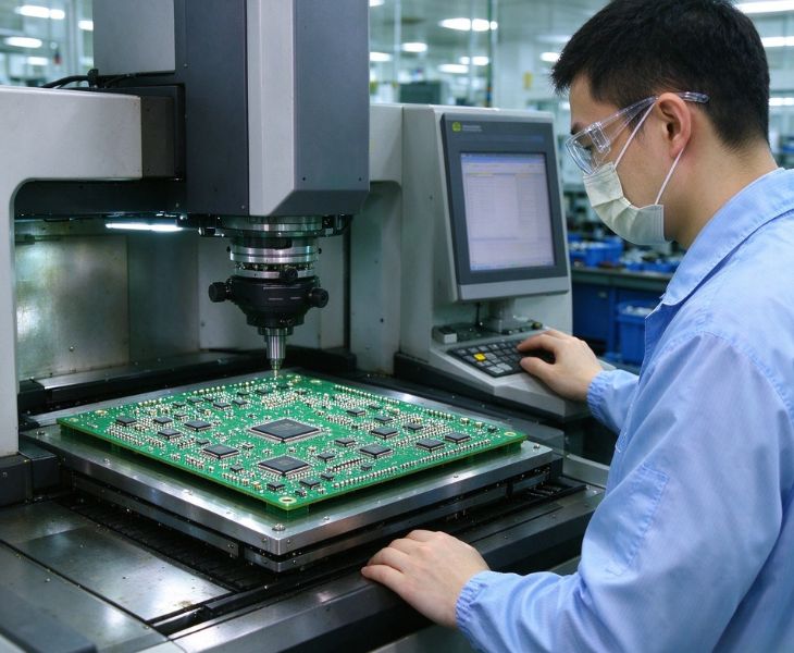
In the AI PCB assembly operation, we use a high-reliability SMT/THT solder joint technology, which meets the requirements of electronic equipment for connection reliability. We strictly control the soldering parameters, solder joint formation, and process consistency during the assembly process of SMT and THT to improve the reliability of electrical and mechanical connections. Combined with automated production and AOI and X-Ray testing, it can identify solder beads, false soldering, insufficient solder joints, solder voids, and hidden connection defects.
Applications of AI PCB
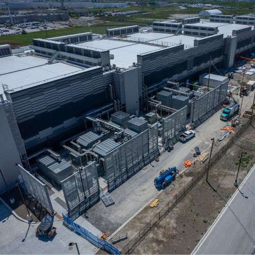
Our AI PCB solutions support high-load AI computing needs, achieve stable power distribution and high-speed interconnection, and help you build a reliable and high-density computing infrastructure that can achieve high availability even when computing density and data traffic continue to grow.

Our AI PCB uses ultra-low loss M9 material and HDI microvias to reduce insertion loss to <0.8–1.0 dB/inch at 112G PAM4, helping to maintain signal integrity in critical connections. We help you optimize the switching matrix, achieve sub-microsecond packet forwarding, and meet real-time inference cluster needs.

For devices facing 400G/800G high-speed Ethernet, our AI PCB provides the 2/2 mil thin line and Dk<3.0 medium material required for high-bandwidth networks, reducing insertion loss to only 0.5 dB/ft, meeting the communication design with high speed and traffic requirements.

For outdoor telecom equipment exposed to extreme temperature changes and constant vibration, we provide PCB materials, assembly processes, and protective solutions selected for the required environmental conditions. Thermal cycling and vibration testing can be arranged according to project requirements.

For data center architectures that require predictable quality and on-time delivery, we design AI PCBs specifically for high-speed signaling, dense interconnects, and high thermal loads, and vertically integrate them from raw materials to finished product assembly, helping you shorten supply chain cycles.

With multi-layer manufacturing, high-density cabling, and one-stop PCBA assembly, we provide a stronger hardware foundation for your enterprise network equipment to meet the ever-upgrading network needs. One-stop manufacturing mode helps you release new switches and routers earlier than your competitors.
More layers can provide more routing channels for high-speed differential pairs, power layers, and ground references, helping to separate critical networks and control electromagnetic coupling. We are able to provide high-layer-count AI and server PCBs with 40+ layers.
But the number of high layers also increases manufacturing complexity and material consumption. For AI network equipment, the number of layers is not always better. The layer number should be determined based on many factors.
We can design multi-layer AI PCBs that support high-density cabling while maintaining controlled impedance and a stable power supply, helping you achieve low-loss, low-latency signal propagation.
High-speed AI network design often requires configuring a dedicated signal layer and setting reference planes at adjacent locations. At the same time, separate power layers and strata enable improved power distribution and provide controlled return paths.
Besides, it is also necessary to comprehensively consider the medium thickness, copper thickness, line width, through-hole structure, and power layer distribution; in particular, high-speed differential signals correspond to being equipped with a suitable reference plane and a stable medium structure to maintain impedance and reduce crosstalk.
Material selection is equally important because the dielectric constant and loss characteristics directly affect signal propagation.
At higher data rates, even small changes in material properties or wiring geometry resulting in small impedance discontinuities can increase insertion loss and reduce signal quality, causing reflections, attenuation, and waveform distortion.
The material selection is very critical for the dielectric constant and dielectric loss factor, which affect signal propagation in PCBs. Excessive traces, unnecessary over-holes, sudden changes in line structure, and improper control of the reference plane can also further degrade signal quality.
We use low-loss materials, impedance control, optimized stacking, appropriate copper surface processing, and high-speed wiring design to help high-speed AI network links maintain stable signal integrity.
When your AI system operates temperature exceeds 100°C or must endure lead-free reflow soldering above 260°C, a high Tg laminate with a glass transition temperature >170°C should be selected.
Higher glass transition temperatures help the substrate maintain dimensional and mechanical stability as operating temperatures rise and reduce the risk of pad pit cracking and overhole cracking during repeated temperature increases and decreases.
High-power AI network devices generate a lot of heat, so high-Tg materials have high application value. At the same time, it can also reduce the risk of plate deformation during lead-free reflow soldering.
For high-current regions, we use suitable copper thickness and sufficient conductive paths to reduce voltage drop and resistive losses. The decoupling element is arranged close to the chip power pin to respond quickly to transient current demands.
We also control the return path, reduce unnecessary over-holes, and isolate the sensitive signal area from the noisy power supply area based on actual conditions, and maintain a continuous reference plane to make the return path more controllable.
For high-power AI network hardware, we combine power distribution analysis with heat dissipation design to control high-current heat generation and achieve a stable power supply.
We will check the wire width and spacing, aperture, aspect ratio, copper thickness, laminated structure, impedance structure, through-hole configuration, solder mask spacing, component spacing, and paneling scheme of the AI PCB before production starts. For high-speed designs, it is also necessary to evaluate the impedance structure with material selection focused on avoiding manufacturing deviations that affect signal performance.
If problems such as wire width or wrong spacing, difficult-to-machine via structures, or inapplicable component packaging occur, we can detect them in advance through DFM review and discuss modifications with you in time, reducing risks such as production defects or rework.
Our quality control of high-level AI PCBs extends from material checks through to final electrical testing. The incoming materials undergo strict verification to check whether the material specifications and the multi-layer pressing process need to control the interlayer alignment, plate thickness, and bonding consistency.
During the production process, critical dimensions are continuously monitored. Automatic optical inspection detects surface defects and line anomalies, while electrical testing is used to verify line conduction and insulation performance. For related PCBA structures, X-Ray can also be used to detect hidden soldering defects. We also keep production records and testing data to achieve product traceability.
We control component quality at the source through qualified supplier management, multi-source qualification certification, and strict incoming material inspection. For critical materials such as ultra-low loss materials, our BOM intelligent system will mark long delivery periods, production stoppages, and high-risk parts in advance, and completely eliminate the single-source risk by pre-certifying alternative materials.
We forecast demand 6–12 months in advance, lock in front-line supplier allocations, and maintain reasonable buffer stocks. This forward-looking strategic procurement and supply chain management ensures that your AI PCBA project can proceed steadily and on time even in the face of industry material shortages.