



Antenna PCB Manufacturer & Turnkey PCBA Supplier
CONSONS manufactures Antenna PCBs with a line width and spacing down to 0.10mm/0.10mm for compact antenna layouts. Controlled impedance supports 50Ω RF signal transmission for Wi-Fi, Bluetooth, 4G/5G, GNSS, IoT, and other wireless devices operating at 2.4 GHz, 5 GHz, and sub-6 GHz.
Our Antenna PCBs use precise circuit geometry, controlled routing, stable dielectric structures, and consistent manufacturing processes to reduce signal loss and impedance variation. As an EMS, ODM, and OEM supplier, we provide PCB manufacturing, PCBA assembly, component sourcing, testing, and final assembly. Streamlined component sourcing, quick-turn CAM processing, and automated SMT lines allow us to deliver complex antenna array prototypes in as fast as 5 business days.
Send your design or RF requirements for a free DFM review and custom manufacturing solution.
Types of Antenna PCBs We Supply
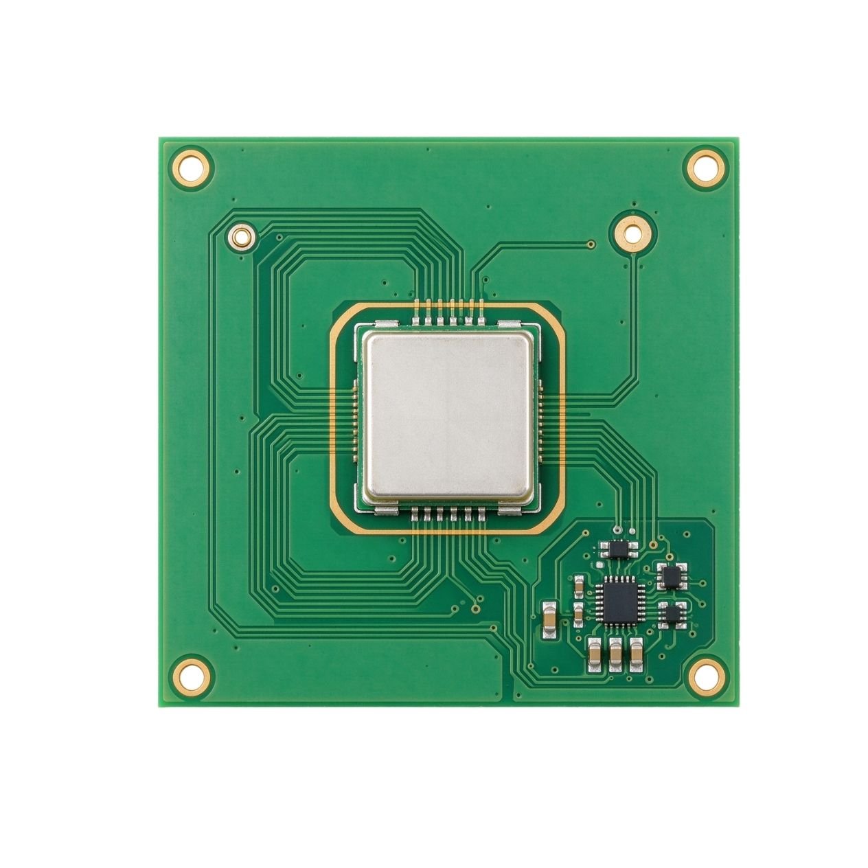
Designed for precise satellite positioning, it supports compact antenna integration and stable signal reception. High-frequency substrates ensure reliable navigation, tracking, and positioning even in harsh urban environments.
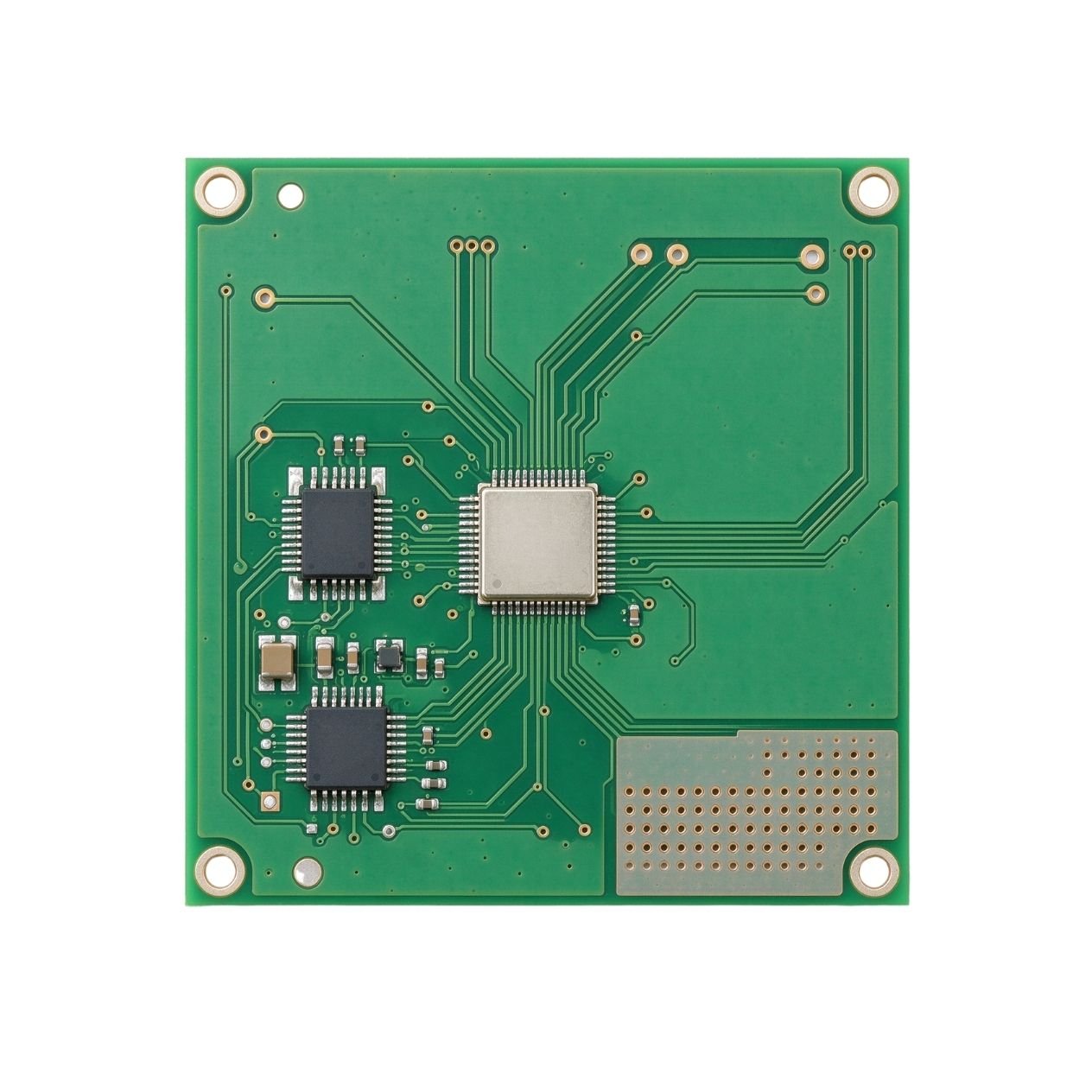
It enables long-range data transmission with ultra-low power consumption, providing rock-solid and highly penetrative wireless connectivity for large-scale, wide-area industrial enterprise networks.

It supports high-speed 4G cellular communication for compact wireless devices. Through high-density layouts, they maintain high-throughput data transmission in space-constrained mobile applications.

It offers an integrated cellular antenna solution compatible with global infrastructure. Suitable for compact designs in tracking and remote communication devices, it delivers stability and cost-effectiveness.
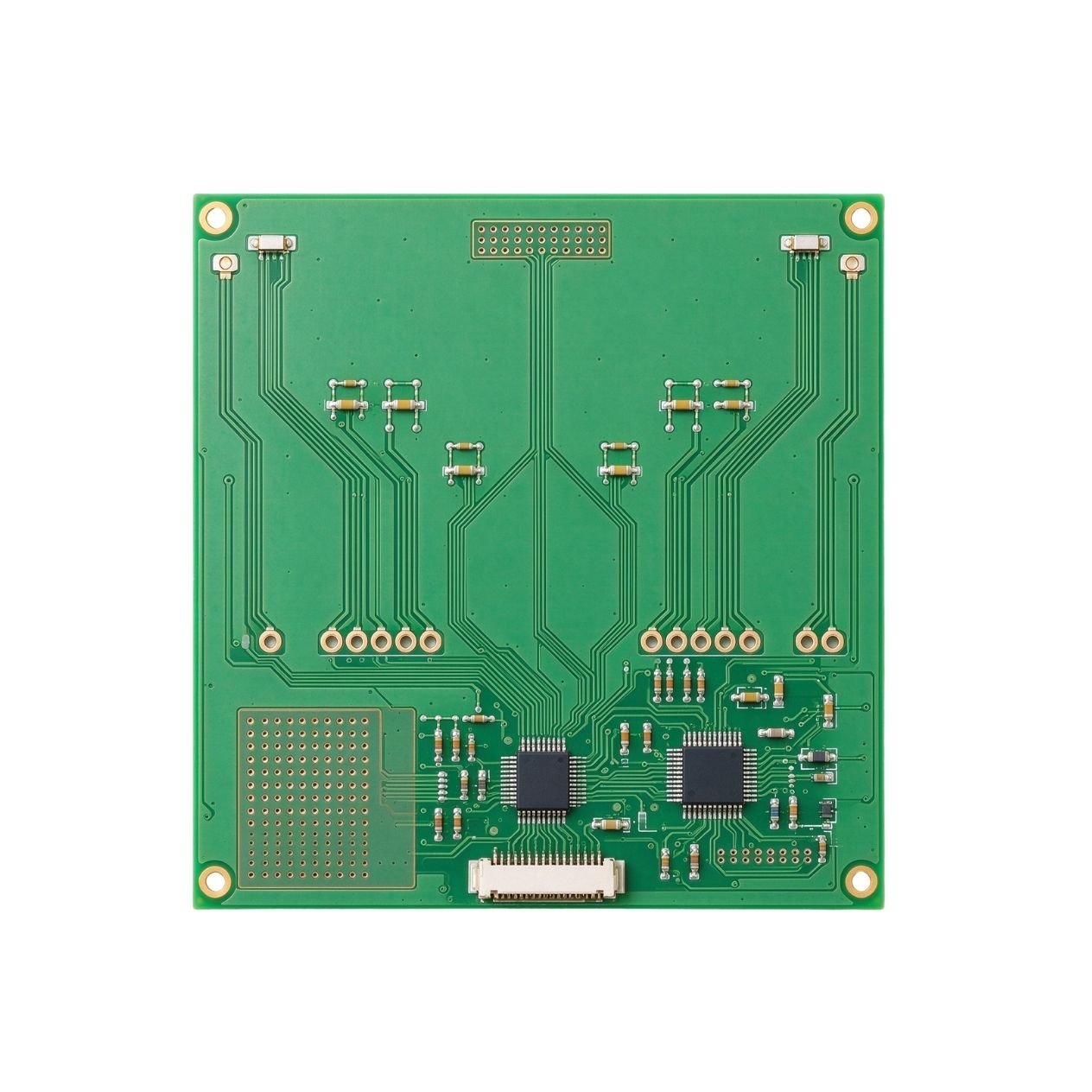
It provides a stable Wi-Fi connection for wireless network products such as routers, access points, smart devices, gateways, etc. The superior multi-band architecture efficiently reduces signal dead spots.
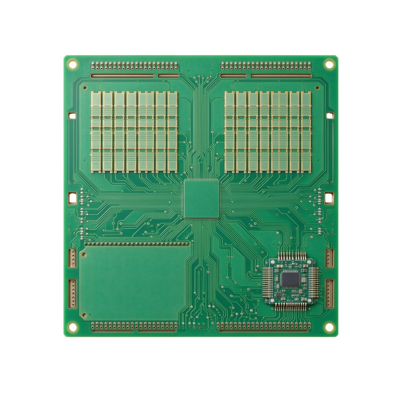
It uses a top-notch millimeter-wave microlayer to release high gigabit speeds. Controlled keep-out zones provide high-speed wireless connectivity for communication equipment, terminals, gateways, and networked devices.
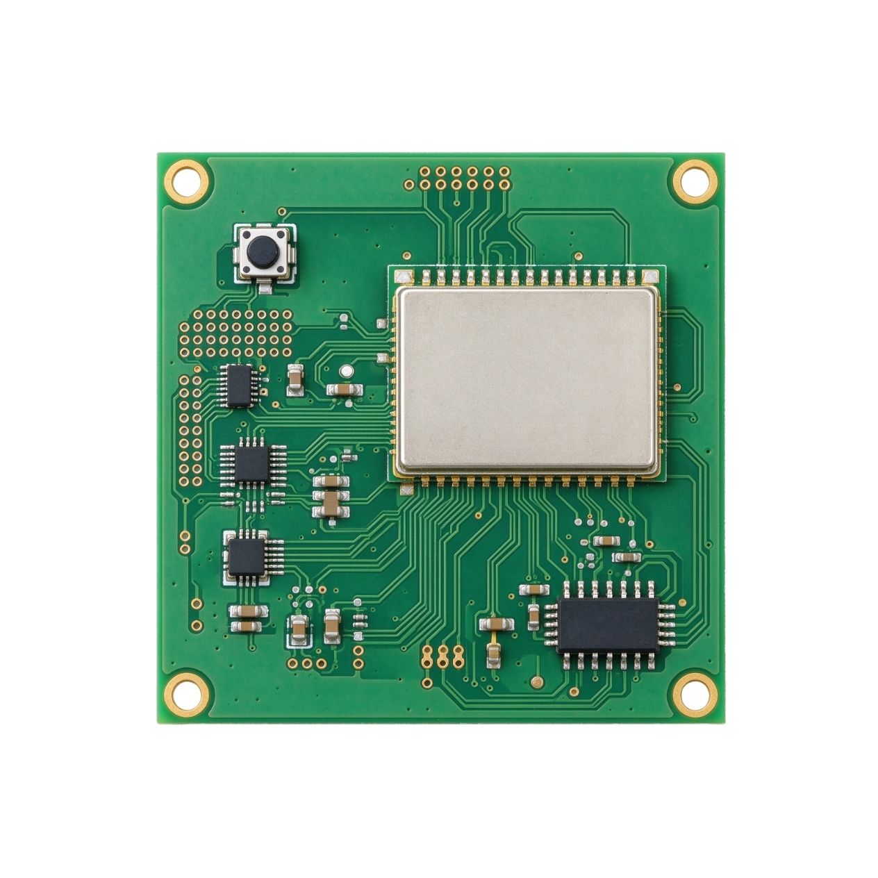
It gives smart sensors continuous narrowband connectivity for years, suitable for compact connected devices. Optimized energy-efficient routing design allows it to achieve reliable cloud-based communications even underground.
Miniaturized Antenna Structures
For wireless products with limited internal space and high antenna performance requirements, CONSONS Antenna PCBs support compact antenna geometries, custom PCB sizes, multilayer structures, HDI layouts, and microvia technology to integrate RF functions into smaller devices. By optimizing antenna placement and surrounding PCB structures, we help manufacturers reduce board space while maintaining key wireless functions. For wearable and IoT devices, we integrate matching networks directly into the antenna layer, eliminating bulky discrete components and further reducing the overall layout size.


Multi-Antenna Integration
We can combine multiple antennas with different frequency bands and functions on a single Antenna PCB. Our 0.6 mm ultra-thin stackup and compact clearance technology reduce electromagnetic interference and improve port isolation, which helps overcome strict space limitations and reduce the required PCB area. Each antenna is independently tuned through automated matching to support multi-band operation. 5G, Wi-Fi 7, Bluetooth, and GPS can be integrated into one layout, helping you achieve multiple wireless functions within limited PCB space.
Antenna Isolation Optimization
When developing an Antenna PCB solution, we consider isolation optimization to reduce unwanted interaction between RF elements. Our proprietary ground-slot patterns and interconnect lines improve isolation between adjacent radiators from 15 dB to above 25 dB, helping address co-site interference. We use full-wave 3D simulation and iterative tuning to suppress surface waves and reduce the envelope correlation coefficient (ECC) below 0.1. Antenna Isolation Optimization is especially important for MIMO and multi-band products that require multiple antennas within limited space.

Applications of Antenna PCB

Smartphone and mobile device manufacturing requires both wireless performance and efficient use of internal space. Our Antenna PCBs integrate antenna structures into compact PCB designs, supporting high-density component layouts, helping you maintain signal strength while developing thinner and lighter devices.

Wearable electronics have limited and irregular internal space, requiring thin and flexible antenna solutions. Our flexible and rigid-flex Antenna PCBs are very thin and have passed over 10,000 bending cycles and maintain stable performance when bending with the enclosure or during repeated movement.

By reducing antenna clearance areas and optimizing internal layouts, we improve PCB space utilization while supporting complex electronic architectures. Our 8-port MIMO arrays provide isolation above 25 dB, maintaining high data throughput in congested situations and delivering reliable Wi-Fi coverage through walls.

To meet the complex RF architectures and compact hardware designs of 5G equipment, our Antenna PCBs use high-density structures with hybrid stackups for complex integration, which helps accelerate 5G equipment development and base station deployment.

Our Antenna PCBs are designed for space-constrained IoT hardware, including smart sensors, gateways, tracking devices, and connected controllers. We provide support to help integrate antennas efficiently, simplify the supply chain, and move from engineering prototypes to stable mass production smoothly.

For GNSS/GPS modules used in positioning devices, trackers, navigation equipment, and location-based electronics, our Antenna PCBs use dual-feed circular polarization with phase center stability < 1 mm. Low-loss PTFE materials reduce signal delay and support sub-meter accuracy in urban environments.

Antenna PCBs for ADAS and automotive radar need to deal with demanding environments. Our Antenna PCBs comply with AEC-Q100 requirements. Microstrip patch arrays achieve ±3 µm copper etching accuracy and 2° angular resolution. Automated assembly and 100% RF testing support reliable ADAS systems.

Our Antenna PCBs integrate wireless antenna structures into compact automotive electronic modules while supporting complex vehicle architectures, reducing assembly complexity, and enabling connected vehicle platforms to maintain communication, navigation, and tracking across different situations.
Choosing the right Antenna PCB requires considering the operating frequency, antenna type, available space, and required RF performance. For demanding RF applications, low-Dk and low-Df materials can help reduce dielectric loss and improve signal performance. For some high-frequency designs, materials with a Dk below 4 and Df below 0.005 may be considered depending on the RF requirements and stackup.
Chip antennas can reduce antenna layout area but may require additional tuning and clearance, while PCB trace antennas can reduce component costs but usually require more PCB space. Multi-band or MIMO products may require multiple antenna structures with proper isolation.
Yes. When the product structure and RF requirements allow, an Antenna PCB can be integrated into the main PCB, eliminating external antenna components and reducing BOM cost, making it suitable for compact wireless devices.
The antenna pattern is placed directly on the same PCB as the electronic circuits, removing the need for a separate antenna in some designs. However, the antenna area must maintain sufficient clearance from copper, batteries, displays, shields, screws, and other conductive structures to control unwanted radiation and coupling.
The ground plane and antenna feed structure must also be properly designed to avoid unnecessary coupling and detuning.
An RF PCB is mainly used to transmit, process, or distribute high-frequency radio signals, while an Antenna PCB specifically includes an antenna structure for transmitting or receiving electromagnetic energy.
An RF PCB may carry RF circuits. An Antenna PCB can use part of its copper pattern as the radiating element and may also integrate RF feed lines and matching circuits. Therefore, an Antenna PCB is an RF-oriented PCB, but not every RF PCB contains an antenna.
Traditional RF PCBs may use external whip antennas or ceramic chip antennas, while an Antenna PCB integrates the radiator directly into the board.
The ground plane is part of the antenna’s electromagnetic environment and is one of the key factors affecting bandwidth, efficiency, and radiation pattern. An undersized ground plane may reduce radiation efficiency or shift the resonant frequency, while a larger ground plane does not always provide better performance.
The optimal ground plane size depends on antenna topology, operating frequency, PCB dimensions, substrate properties, and nearby components. During Antenna PCB development, we evaluate the ground plane together with the antenna geometry rather than treating it as an independent layout area. Prototypes and RF testing are then used to verify actual performance.
Ground clearance is important because conductive materials placed too close to a PCB antenna can change its electromagnetic field distribution and electrical characteristics. Proper clearance helps the antenna maintain its intended operating characteristics and reduces unwanted interaction with surrounding circuits.
There is no universal clearance value, but a clearance of at least 3 mm is recommended in many applications. Clearance also affects impedance bandwidth, with larger clearance generally providing wider bandwidth.
For short-range communication, reducing clearance can save PCB space while meeting performance requirements. For optimal results, ground clearance should be considered on both outer and inner layers.
Antenna detuning occurs when changes around the antenna shift its intended resonant characteristics, which is usually caused by nearby metal components. Changes in PCB dimensions and geometry can also affect resonance.
Manufacturing tolerances may further contribute when the antenna structure is sensitive to dimensional changes. Detuning can weaken wireless performance. To reduce this risk, we need to understand the complete product environment, not just the PCB.
The enclosure, battery, display, mechanical components, cable positions, and other conductive structures should be considered during antenna development. Prototype testing and RF validation can then confirm the required performance in the final product.
Impedance matching is important for transferring RF energy efficiently between the transmitter, transmission line, matching network, and antenna at maximum available power. When impedance is mismatched, part of the RF energy is reflected toward the source instead of reaching the antenna.
These reflections create standing waves on the transmission line, reduce signal integrity, and may interfere with other parts of the PCB. Excessive reflection increases return loss, reduces actual transmitted or received power, and affects wireless performance. Poor matching can also reduce effective radiated power, while a well-matched antenna can radiate more energy with the same input power.