



Your Trusted Sensor PCB Manufacturer in China
- Manufacturing Precision:Consons sensor PCBs offer 0.1 mm min line/space and 0.1 mm min vias, enabling high-density routing for compact sensor modules.
- Board Thickness: 0.2–2.0 mm PCB thickness, fitting diverse space, strength and lightweight design needs.
- Impedance Control: 50Ω/75Ω/90Ω single-ended, 100Ω/120Ω differential impedance, tolerance ±5%.
- Copper Weight & Thickness: Copper thickness 0.5–3 oz, selectable based on current load, signal loss and thermal needs.
- Surface Finish: HASL, ENIG, ENEPIG, OSP options for reliable soldering, stable contact and oxidation resistance.
- Certification: ISO 9001, IATF 16949, ISO 13485 certified; compliant with UL, RoHS and REACH.

Our Types of Sensor PCBs

Through signal transmission and thermal management design, temperature changes are logged and transmitted to control systems, achieving temperature monitoring.
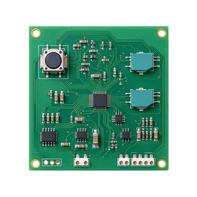
Designed to detect changes in gas or liquid pressure, utilizing high-precision signal processing and transmission to provide consistent pressure monitoring.

Featuring accurate component layout and low-noise design, it facilitates Hall sensors to stably capture changes in magnetic fields, realizing position, speed, and current detection.

Employing an optimized capacitive sensing layout and EMI protection, it supports the acquisition of human touch signals to accomplish highly sensitive interaction control.

By adopting a compact and low-power design, it enables real-time motion data acquisition and satisfies wireless communication needs, suitable for mobile device applications.

The optical layout and signal isolation design minimize the influence of environmental light and EMC interference, enhancing the accuracy of IR signal capture.
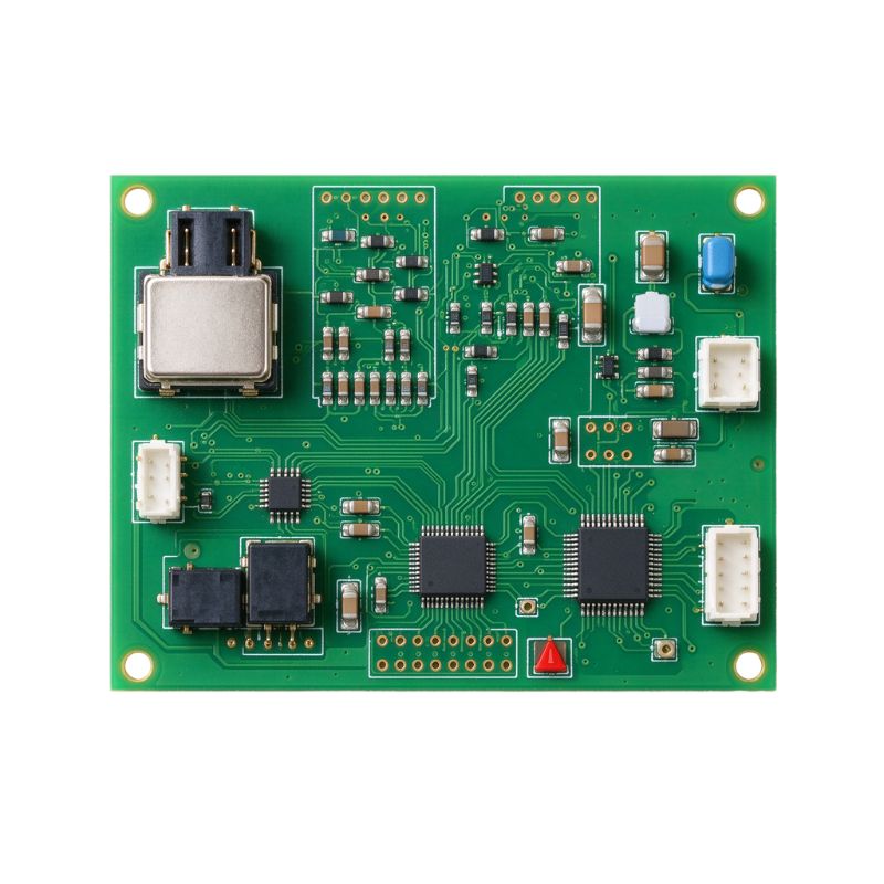
High-sensitivity signal acquisition and environmental protection design, supporting gas concentration monitoring, ideal for air quality assessment and industrial safety inspections.

Ultra-compact size and highly integrated architecture enable the incorporation of micro-MEMS sensors and deliver high-precision signal transmission.
Advantages of Consons Sensor PCB

For thermal cycling conditions, we have implemented a design utilizing low CTE and high Tg materials, supporting operation in a wide temperature range from -40°C to 125°C.

Employing a vibration-resistant and shock-resistant design, meeting the demands of a broad frequency spectrum of 10Hz–2000Hz, and remaining consistent during long-term operation

Supports nV/μA level transmission, utilizing low-loss circuit design and refined electrical control to minimize signal attenuation and improve measurement accuracy.

The design incorporates digital signal isolation, differential signaling, and ground shielding to decrease crosstalk and noise disturbances, improving detection precision of 30%.

Offers precise impedance control to optimize signal integrity, reduce reflection and loss, and address the needs of sensitive sensor signals and high-speed interface transfers.

By utilizing signal isolation, grounding design, and EMI shielding methods, the effects of EMC interference and crosstalk are diminished, improving stability in complex environments.
Customized Sensor PCB Solutions
Consons provides customized sensor PCB solutions to meet your sensor demands, product design, and applications. In functional customization, we integrate multiple sensor types like
temperature, pressure, optical, gas, and MEMS sensors, while enabling customization of signal conditioning, signal amplification, A/D conversion, and communication interfaces. In structural adaptation, we offer customization of PCB forms, flexible structures, mounting positions, and assembly methods to help your sensor PCBs better integrate into devices. Through these versatile customization options, we can help you maximize product integration and accelerate the process.
Sensor PCB Quality Assurance
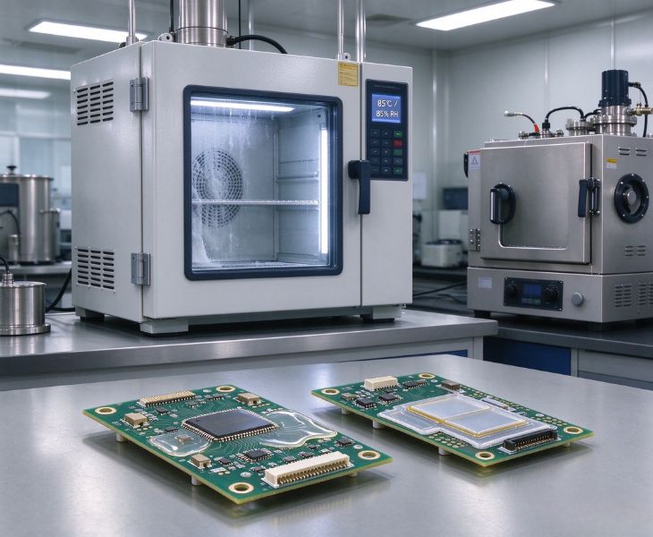
We deliver three-proof coating, moisture-resistant coating, and sealed protection designs to safeguard the durability of your sensor PCB projects. These solutions improve long-term stability in environments with high humidity, corrosion, and temperature fluctuations. Depending on project specifications, we also offer humidity and heat testing at 85°C/85% RH, 48-hour salt spray testing, and insulation performance testing. In addition, we support testing including thermal cycling, vibration, impedance, and signal accuracy calibration, and supply corresponding test reports. These certifications help you assess the feasibility of sensor PCBs in practical environments, lowering product development risks.
Why Choose Consons As Your Sensor PCB Partner?


- Professional Manufacturing Experience: With over 20 years of experience in sensor PCB manufacturing, Consons supports you from prototype validation to high-volume production, helping you quickly accomplish PCB project launches.
- PCB Assembly Services: We have 15 SMT production lines and 4 DIP production lines, which can provide you with complete sensor PCB assembly services to help you streamline the supply chain and shorten overall project lead times.
- Fast Technical Support: Consons has 35,000 square meters of production facilities and more than 1,600 skilled employees. They can assess and handle your sensor PCB projects rapidly.
- Global Delivery Capability: We have worked with more than 40 countries, have ample overseas sensor PCB project experience, and are familiar with international technical documentation and export procedures.
Our Sensor PCB Specification
| Category | Parameter | Capability & Specification |
| Board Structure & Layers | PCB Type | Rigid, Flexible, Rigid-Flex, HDI |
| Layer Count | 1 – 40 layers (Rigid); 2 – 12 layers (Rigid-Flex) | |
| Board Thickness | Standard: 0.4mm – 3.2mm (Custom up to 6.0mm, tolerance ±10%) | |
| Precision & Micro-Machining | Min. Line Width / Spacing | 3.74mil / 3.74mil (0.095mm / 0.095mm) |
| Min. Hole & Via | Mechanical Hole: 0.10mm | Laser Microvia: 0.10mm | |
| HDI Structure | 1+N+1, 2+N+2 build-up; Blind via, Buried via, VIPPO (Via-in-Pad) | |
| Material & Copper | Base Material | FR-4, High-Tg FR-4, Polyimide, Rogers, Halogen-Free Laminate |
| Copper Thickness | 0.5oz to 3oz (18μm – 105μm); 2oz as standard | |
| Electrical Performance | Controlled Impedance | 50Ω, 75Ω, 90Ω (Single-ended); 100Ω, 120Ω (Differential) Tolerance: ±5% (High-precision) / ±10% (Standard) |
| Surface Finish | ENIG, ENEPIG, OSP, Immersion Ag, Immersion Sn, LF HASL | |
| Assembly & Packaging | Sensor Package Support | LGA, QFN, 0.25mm-pitch BGA, MEMS, PoP, COB |
| PCB Assembly (PCBA) | SMT (Supports ultra-fine 01005), THT/DIP, Selective Soldering | |
| Conformal Coating | Acrylic, Silicone, Polyurethane, Parylene (Customizable) | |
| Quality & Compliance | Inspection & Testing | 3D AOI, 3D SPI, X-Ray, Flying Probe E-Test, ICT, FCT, Burn-in Test |
| Quality Standard | IPC-6012 & IPC-A-610 (Class 2 / Class 3) | |
| Compliance Certs | RoHS 2.0, REACH, UL 94V-0, Halogen-Free, IATF 16949, ISO 13485 | |
| Volume & Delivery | Production Volume | Prototype (No MOQ) to High-Volume Mass Production (Million-level) |
Where Are Consons’ Sensor PCBs Applied?

Our sensor PCBs work well in BMS battery monitoring systems, TPMS tire pressure monitoring devices, and ADAS sensor modules. These PCBs are built with excellent vibration resistance, temperature tolerance, and environmental adaptability, while also strictly complying with IATF 16949 quality management standards.

We specifically design sensor PCBs for industrial robots, PLC control systems, and automated inspection equipment. Its outstanding electromagnetic compatibility and wide operating temperature range can minimize the influence of EMC interference and temperature fluctuations on signals, helping equipment sustain consistent data collection.

To meet the demands of IoT devices for low power consumption, compact structure, and reliable signal transmission, our sensor PCB utilizes a high-density and miniaturized design to facilitate the integration of numerous sensors and wireless modules. Ideal for intelligent home devices, environmental monitoring systems, and others.

We provide sensor PCBs for drones, avionics, and satellite communication systems. These PCBs are designed using low CTE and high Tg, offering exceptional vibration resistance and reliability to satisfy the needs of long-term operation at high altitudes and low pressures.

In BMS, energy storage systems, and new energy vehicle charging equipment, real-time collection of voltage, current, and temperature data is important for safeguarding system safety. Consons sensor PCBs support high-precision signal acquisition and dependable electrical design, helping new energy equipment realize stable data monitoring.
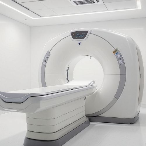
Our sensor PCBs are also widely used in patient monitoring devices, wearable medical devices, and diagnostic instruments. Their high-density wiring capability supports compact and lightweight designs while meeting the flexibility and durability requirements of specialized equipment.
Consons Sensor PCB Manufacturing Process
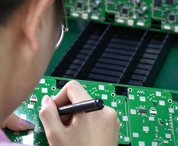
We strictly manage every stage of the sensor PCB manufacturing process in compliance with IPC Class 2 and Class 3 standards to guarantee that all products have reliable performance.
Explore Our Sensor PCB Boards

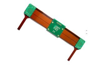


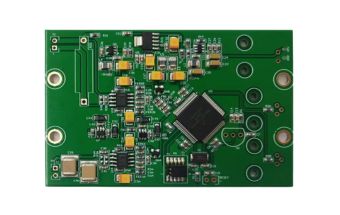
A sensor PCB is a type of printed circuit board specifically designed to incorporate sensors and other electronic components. It provides the necessary electrical connections to transmit and handle signals from the sensors. Depending on design requirements, this type of PCB can also integrate functions like power management, signal processing, and communication circuits. Sensor PCBs support a wide variety of sensor types and can be customized in size, structure, and layout to meet particular sensing and control demands.
Consons offers Standard FR-4, High-Tg FR-4, Polyimide (PI), and high-frequency laminates. These materials have different characteristics in thermal resistance, flexibility, and electrical performance. This table helps you choose the proper material for your project.
| Material | Key Characteristics | Best For |
| Standard FR-4 | Cost-effective, stable, easy to process | General sensor PCB designs |
| High-Tg FR-4 | High heat resistance, good dimensional stability | High-temperature environments |
| Polyimide (PI) | Flexible, lightweight, bend-resistant | Flexible & compact designs |
| High-Frequency Laminates | Low loss, stable Dk/Df | High-frequency & RF signals |
We have several methods to mount sensors on a PCB according to your sensor’s package type, size, and application requirements.
- SMT: Suitable for small sensors in QFN, LGA, BGA, and MEMS packages.
- THT: Provides a reliable mechanical connection for sensors with leads.
- Connector/Socket: This enables easier replacement and maintenance of sensors.
- COB/Wire Bonding: Supports direct integration of the chip with the PCB and is used for microsensor modules.
Our sensor PCBA process involves mounting and soldering sensors and other electronic components onto a printed circuit board, then conducting inspections and tests to verify correct assembly.
The standard procedure is as follows:
- Solder Paste Printing
- Sensor & Component Placement
- Reflow Soldering
- THT / Special Sensor Assembly
- AOI & X-Ray Inspection
- Electrical & Functional Testing
- Conformal Coating (Optional)
- Final Inspection
We decrease noise and signal interference in sensor PCBs through reasonable grounding design, signal routing, power filtering, and separation of sensitive analog signals from high-speed or high-current circuits. When necessary, we can also use a ground plane and a shield to improve signal stability.
Before production, we review your PCB files to help you avoid potential grounding issues, signal routing problems, and manufacturability concerns. Additionally, to address your design specifications, we can optimize the layer stackup and control impedance to safeguard the steady transmission of signals.
Yes. We can manufacture HDI boards and rigid-flex sensor PCBs designed for miniaturized, high-density sensor systems.
Our HDI process capabilities include micro-vias, blind/buried vias, in-pad vias, and 1+N+1 and 2+N+2 layer structures.
For rigid-flex sensor PCBs, we support combined rigid and flexible areas in a single-piece design, minimizing connector count and making sensors adapt to tight spaces.
We can also provide manufacturability analysis and assessment services tailored to your project.
First, you need to choose the PCB layout after considering installation space and operating conditions.
For standard sensor modules, use rigid sensor PCBs; for confined or curved spaces, employ flexible sensor PCBs; and for situations requiring both component support and flexible interconnects, rigid-flex sensor PCBs are the best choices.
Second, clearly define the circuit density you need.
For sensor modules that require fine-pitch components and have limited routing space, HDI sensor PCBs can achieve higher interconnect density.
Finally, you should determine the sensor signal type and sensitivity demands.
Low-level analog signals require careful grounding and shielding; high-speed signals must achieve controlled impedances.
Ready to Discuss Your Sensor PCB Project?
Whether you need standard specifications or customized sensor PCBs, our team can provide you with end-to-end services from prototype design to mass production.