



Reliable Switch PCB Solutions Supplier for Communication Networks
CONSONS Switch PCB supports customized designs with up to 32 layers and single-channel transmission rates of up to 112 Gbps. It is designed for high-speed signal routing, impedance control, grounding, and power distribution to support stable data transmission under high network loads. It is suitable for Ethernet switches, data center switches, industrial network switches, and telecom equipment.
As a one-stop EMS, ODM, and OEM supplier, CONSONS integrates Switch PCB manufacturing, assembly, testing, and packaging into one process, which reduces delivery time from prototypes to mass production and simplifies supplier coordination. We manufacture according to IPC-6012 Class 3 standards and use AOI, X-ray inspection, and functional testing to control quality and support consistent production.
Contact us today for a custom Switch PCB solution for communication networks.
Switch PCB Types
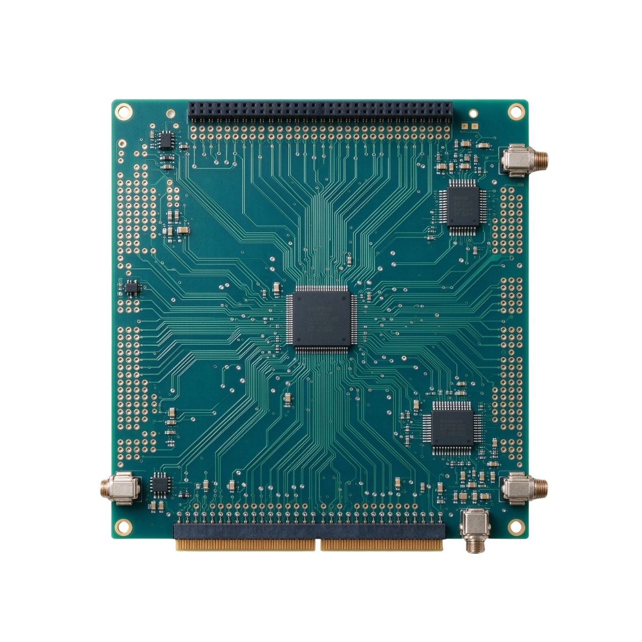
It supports high-speed data transmission. The optimized routing architecture reduces signal loss and crosstalk, ensuring its stable operation under high-bandwidth network traffic.

It supports high component and interconnect density within limited board space, supporting devices with compact layouts, multiple interfaces, and complex network hardware designs.

It uses microvias, stacked vias, and fine lines to achieve dense routing for high I/O counts in tight areas, which is needed for advanced switch ASICs and multi‑layer interconnects.

The impedance is precisely controlled within ±5% across high-speed signal paths to reduce reflections, preserve signal integrity, and support consistent network transmission.

The low-loss materials and specially designed routing enable it to support high-frequency signal transmission and provide stable electrical performance for high-density telecom deployments, like 5G backhaul applications.

It integrates digital, analog, and power circuits on one board with dedicated layout strategies and isolated planes to prevent noise coupling and support accurate signal conversion.
Low Insertion Loss
CONSONS Switch PCB uses low-loss materials, with optimized dielectric thickness and copper surface roughness, helping keep signals stable over longer paths. The configuration keeps stable electrical performance across key high-speed signal paths and helps network switches preserve signal over longer paths. We support designs with up to 32 layers and single-channel transmission rates up to 112 Gbps. Low insertion loss makes our switch PCB suitable for Ethernet switches, data center switches, telecom equipment, and other high-throughput communication network systems.


Reduced Crosstalk
Our layout separates sensitive signal paths from interference sources and provides defined return paths for critical signals. Controlled differential-pair routing, optimized trace spacing, and grounded via fences limit coupling between adjacent high-speed circuits. Dedicated ground planes create a stable reference path, while layer allocation helps isolate sensitive signals from noisy power circuits. We control spacing and impedance during manufacturing, further limit noise coupling, while preserving signal quality across dense routing areas. This design supports stable data transmission in mixed-signal environments.
Applications of Switch PCB

Data center equipment should handle high port density and continuous data traffic. Our Switch PCB supports 112 Gbps single-channel transmission, insertion loss below 0.8 dB/in, and crosstalk below -50 dB, reducing bit errors. It increases throughput and helps lower your infrastructure costs.
Our switch PCB provides stable circuit performance for telecom equipment handling large network traffic. Controlled impedance and low-loss materials preserve signal quality across long-distance links. The board also withstands temperatures of -40°C to +85°C and high humidity, helping reduce field failures.
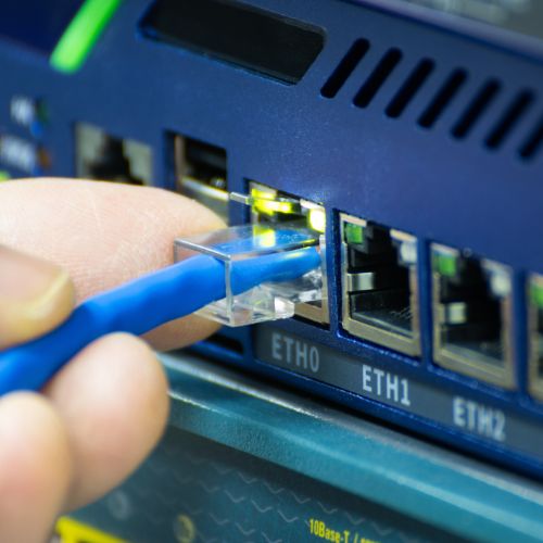
For industrial automation equipment and systems, our switch PCBs provide optimized signal paths to deliver real-time control data to actuators with low jitter. Their reliable structure withstands shock, vibration, and dust, helping reduce unplanned downtime, production losses, and maintenance costs.
For DWDM transceivers and ROADM equipment, our switch PCB supports the electrical interfaces and signal routing. Tight 50Ω/100Ω impedance control reduces signal distortion, allowing optical transceivers to extend rated distances, helping reduce repeater requirements, and lowering fiber network expansion costs.

Our switch PCB handles line-rate packet inspection with deterministic jitter below 5 ps. Low crosstalk and reduced reflection support fast security rule execution, helping maintain full throughput even during DDoS attacks while providing stable network protection without sacrificing performance.
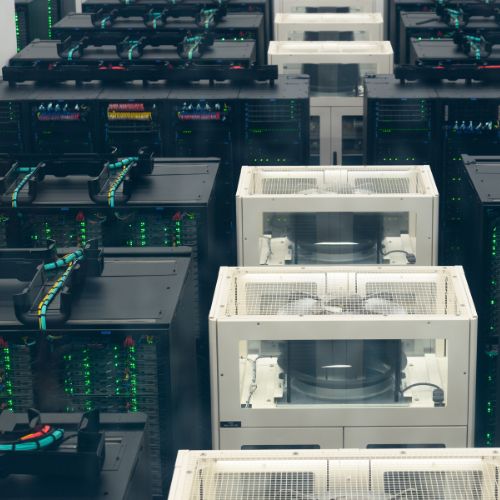
For hyperscale server clusters and storage networks, our high-density switch PCB supports high-density 400G/800G network architectures. Optimized power distribution helps reduce energy consumption, while reliable operation supports smooth cloud expansion and lowers operating costs per Gbps.
A PCB’s dissipation factor (Df) indicates how much electrical energy the dielectric material converts into heat during signal transmission. A lower Df generally means lower dielectric loss, which helps reduce signal attenuation in high-speed Switch PCBs. This becomes more important as transmission frequency and data rate increase.
For communication network switches, low-Df materials help maintain high-speed signal integrity and reduce cumulative transmission loss. Standard FR-4 has a Df of about 0.020 and can produce approximately 1.5–2.0 dB/cm of dielectric loss at 10 GHz. We select PCB materials based on your required data rate and electrical performance.
Designs using high-end switching ASICs may require 20-30+ layers depending on BGA density, SerDes routing requirements, power distribution, and board dimensions. 400G/800G switch designs may use higher layer counts to accommodate dense high-speed routing and power delivery requirements.
More layers provide additional routing space for high-speed differential pairs, power planes, ground planes, and signal isolation. A properly designed multilayer Switch PCB reduces routing congestion and provides more controlled signal return paths.
However, increasing the layer count also increases manufacturing complexity and cost. The appropriate layer count depends on component density, PCB size, impedance requirements, and power demand.
FR-4 can be used for network Switch PCBs when the required transmission rate, operating frequency, PCB structure, and electrical performance remain within its practical range. Standard FR-4 provides good mechanical strength, manufacturability, and cost efficiency, making it suitable for many conventional network switching applications.
However, standard FR-4 is generally better suited to control circuits and lower-speed interfaces below 1 GHz. At higher frequencies, dielectric loss increases significantly. For high-speed or high-frequency designs above 10 Gbps, low-loss laminates may provide better performance through lower Dk and Df values. We can evaluate your design requirements and select the appropriate PCB material.
Yes. We provide multiple lead-free surface finish options that support RoHS and WEEE requirements. ENIG is commonly selected for 400G/800G switch boards for its flat and uniform surface that supports fine-pitch BGA packages. Lead-free HASL can be used for applications with less demanding surface flatness requirements.
ENEPIG is available for designs that require additional gold wire bonding capability. We also support high-Tg materials suitable for lead-free assembly processes. Strict process control helps maintain stable soldering quality for network switches with high component density and reliability requirements. All surface finishes are tested for solderability and reliability to support telecom-grade operation.
When total heat generation is high, but the available cooling area is limited, excessive heat flux can cause rapid overheating. For high-current power rails, using less than 2 oz of copper can increase conductor resistance and heat generation, adding more heat to components.
The area directly beneath BGA chips is a key thermal path. If the thermal via array is insufficient, heat can remain around the chip instead of transferring to inner copper layers or a heatsink interface. Other causes include insufficient airflow inside a 1U chassis and a stackup that places power planes too far from heat-generating layers.
High-current designs require wider traces, thicker copper, and careful thermal planning. For Switch PCBs carrying high-power processors, switching ASICs, or power modules, we consider current distribution during stackup and layout design and use IPC-2221 and IPC-2152 as references for current-carrying calculations.
High-current designs may also require multiple parallel vias to distribute current into power planes, thicker copper on power layers, dedicated low-DC-resistance power planes with a target below 50 mΩ, and thermal-relief pad designs that balance solderability with heat transfer. These factors are incorporated into the design rules to maintain reliable power delivery without compromising signal integrity.
Our Switch PCB uses HDI structures with laser microvias and stacked vias to create additional routing capacity without significantly increasing board dimensions. Thinner dielectric layers can maintain impedance while creating more routing channels.
Advanced packaging and interconnect technologies can further increase component density and routing flexibility within compact board designs. We use fine-line etching and optimized layer allocation to provide dedicated signal, power, and ground layers.
Careful component placement separates high-speed signals, power circuits, and sensitive components to reduce interference. Our designs can route hundreds of differential pairs within a standard 1U form factor while maintaining the required electrical performance.