



Precision RF PCB Manufacturing & Assembly
CONSONS provides precision RF PCB manufacturing and assembly services. We support 1–30 layer rigid PCB structures and 1–8 layer flexible/rigid-flex structures, and use advanced materials such as Rogers/Taconic RF boards to manufacture RF circuit boards, ensuring stable signal transmission in harsh environments. They are widely used in communication equipment, industrial electronic products, high-performance electronic systems, and other fields.
Delivering high-precision RF PCBs with trace/space down to 3.5/4 mil, micro-vias down to 0.15mm, and strict impedance tolerance within ±5%. CONSONS supports your project seamlessly from new product introduction to high-volume manufacturing. At the same time, our engineering team provides in-house DFM analysis and optimized BOM sourcing, which can help you reduce development risks and control manufacturing costs.
Contact CONSONS today for custom RF PCB solutions and quick quotes.
Products by Features

It offers excellent mechanical strength and stable signal integrity for high-frequency electronic applications like base stations or automotive radar.

High-frequency flexible & rigid-flex PCBs featuring controlled-impedance polyimide substrates for dynamic flexing applications. They are suitable for compact electronic systems with complex layouts.
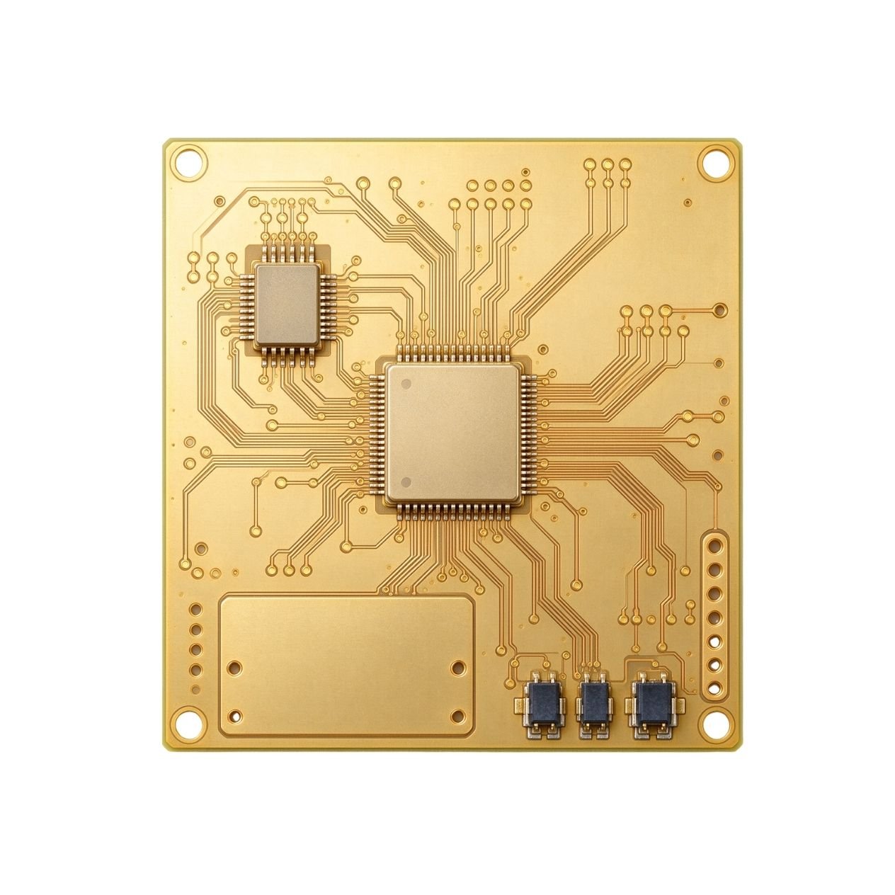
It replaces the thicker magnetic nickel layer in traditional ENIG with an ultra-thin nickel layer plus a palladium barrier layer. The ultra-flat gold surface with Ra<0.1μm minimizes signal scattering.
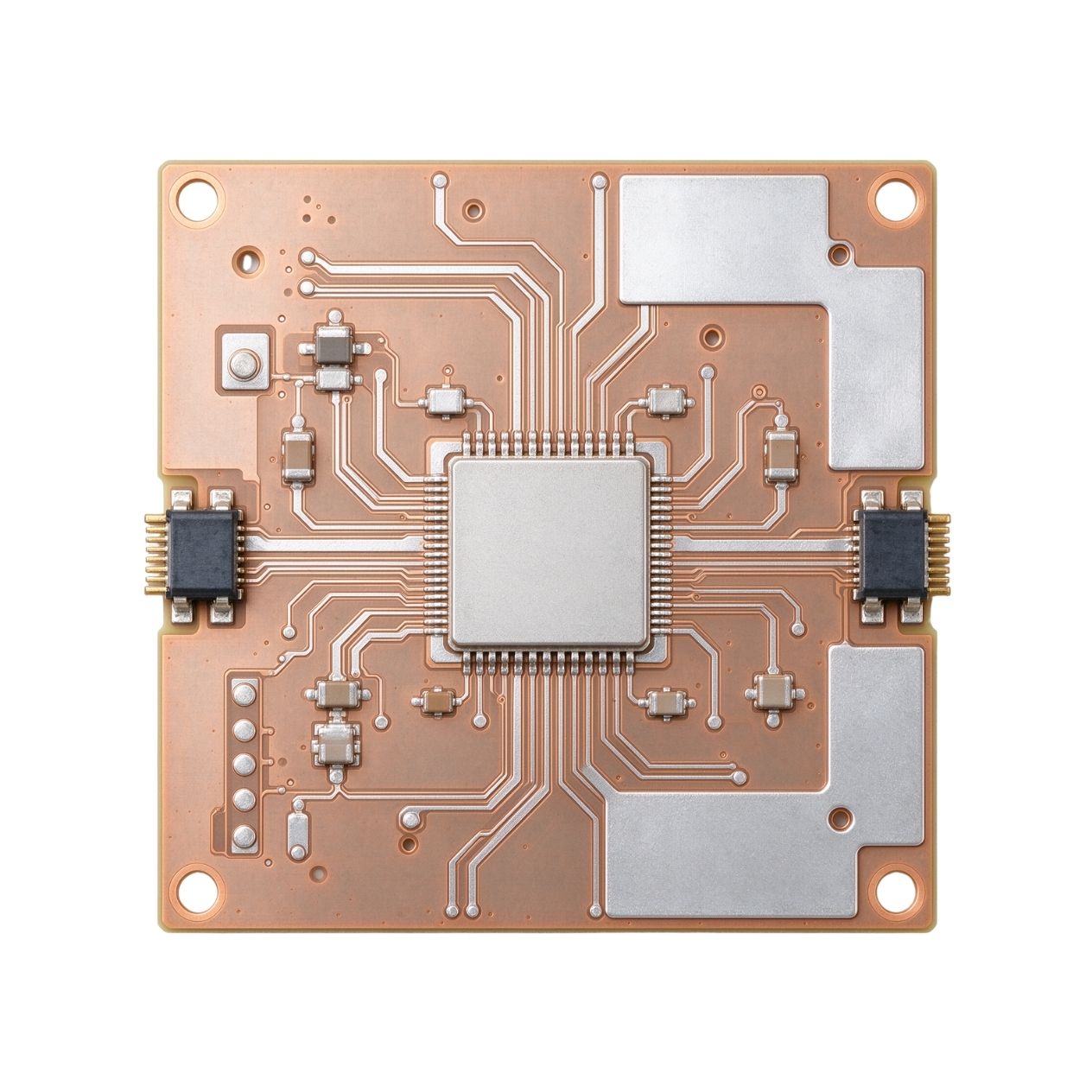
It deposits 0.15-0.4μm pure silver directly on the copper surface. With silver’s excellent conductive properties, it achieves an insertion loss ratio 30-34% lower than ENIG above 25GHz.

It uses Rogers high-frequency laminates, delivering low-loss, stable dielectric constant across a wide frequency range for demanding RF circuit designs.

The Taconic high-frequency PTFE materials provide high stability and low dissipation factor for RF applications requiring precise circuit control, like satellite communication systems.
Advanced RF Material Compatibility
CONSONS supports advanced high-frequency substrates, including Rogers RO4000 and RT/duroid series, Taconic TLY and TSM laminates, PTFE-based materials and high-Tg FR4, with dielectric constants ranging from 2.2 to 10.2. Our hybrid stacking technology can cleverly combine a low-loss signal layer with a cost-effective FR4 ground layer, reducing material costs by up to 30% while ensuring high Dk stability over a wide temperature and frequency range. We also provide material substitution analysis if you need economical solutions.


Precision Multilayer Manufacturing
We have extensive experience in manufacturing multi-layer RF PCBs. The interlayer alignment tolerance is strictly controlled within ±2mil. The production line can achieve a minimum line width of 3.5/4mil and a minimum drilling diameter of 0.15mm. The advanced lamination process we use, combined with precise temperature and pressure control, eliminates delamination and cavitation and ensures the uniform thickness of each layer. Strict manufacturing tolerances ensure full-board impedance consistency within ±5%, resulting in a reliable 50Ω transmission line.
Enhanced Signal Integrity Protection
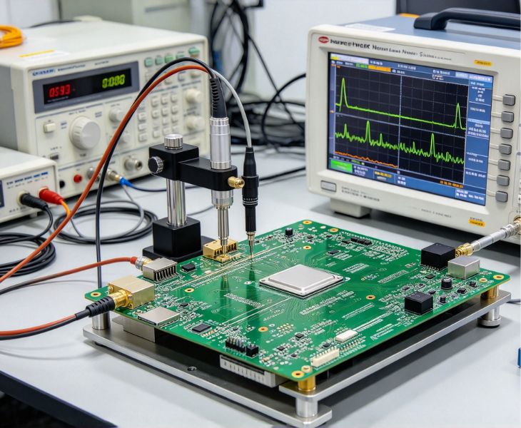
Our design helps high-frequency electronic systems protect signal integrity by ±5% impedance control, precise differential pair routing, and reducing crosstalk through properly spaced and grounded coplanar waveguides. We use TDR testing for impedance verification and a network analyzer to measure the S-parameters and insertion loss of key traces, ensuring that the insertion loss is less than 0.5 dB/inch at a frequency of 10 GHz. We also apply EMI shielding techniques such as via stitching to reduce sensitivity.
Why Choose Our RF PCB Service


- ISO9001 & ISO14001 certified quality systems.
- 4.5 Billion SMT Points Monthly Capacity.
- Extensive collaborating experience with leading component suppliers worldwide.
- 18+ years EMS experience with deep technical expertise.
- 35,000㎡ fully equipped electronic manufacturing facility.
- 500+ skilled professionals support your projects.
Applications of Our RF PCB Products

From high-frequency satellite transponders to advanced telemetry systems, our RF PCB products can transmit signals stably in extreme thermal shock and radiation environments. With strict quality control, our products ensure uninterrupted signal transmission, helping you better complete your space projects.

For massive MIMO base stations and small cells, we provide multi-layer RF PCBAs with extremely low media loss, which can maximize data throughput and significantly reduce latency, supporting 5G infrastructure and wireless devices. With rapid prototyping and production, we help accelerate your 5G rollout.
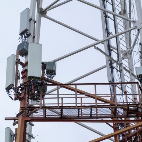
Modern wireless communication devices rely on RF PCB technology to achieve signal processing. From enterprise routers and 5G gateways to point-to-point radios and base station transceivers, our high-frequency PCBAs deliver ultra-low signal loss and superior SNR performance.

Industrial control systems place greater emphasis on maintaining durability in a continuous operating environment. Our RF PCB circuit boards are field proven to withstand extreme conditions like severe electromagnetic interference, high humidity, vibration and extreme temperatures without performance drift.

We can help you develop IoT and smart devices that capture market development trends. Flexible and rigid RF PCBAs allow 3D integration can achieve small product sizes without sacrificing performance. We can also help you extend your product’s battery life and wireless RF range.
High-frequency signals decay fast in ordinary PCB materials like epoxy resin and cannot maintain integrity, while RF PCBs are specifically designed to handle rapidly changing signals. Our RF PCBs use low-loss dielectric materials such as PTFE, Rogers, or ceramic-filled hydrocarbons, which can reduce insertion loss and signal attenuation.
Controlled impedance transmission lines ensure power transfer from source to load by preventing reflections. Copper foils with a smooth surface are used to prevent loss caused by high-frequency current flowing on the surface. Structural designs bind electromagnetic waves tightly inside the trace and substrate to prevent signals from crosstalk with each other.
If dielectric constants of materials change dramatically with temperature, the impedance of the RF transmission line will deviate, causing severe signal reflection.
The sheet without moisture resistance will make the RF signal attenuate a lot in the transmission line in a humid environment, or even cause the sensitive RF front-end circuit to be unable to receive the signal. Some low-end resin materials will age over time, causing electrical properties to deteriorate.
Our RF PCBAs use reliable materials, giving them great impedance between -55°C and +125°C. They maintain almost exactly the same electromagnetic characteristics as new after long-term service.
The RF PCB impedance is directly related to the ground plane. If the ground plane is uneven, it will cause drastic impedance fluctuations. If the ground plane is discontinuous, the high-frequency return current is forced to take a long way, causing the signal to be severely distorted and triggering severe electromagnetic radiation.
In a multilayer RF PCB, a complete ground plane can isolate the signals above and below it. For example, by inserting a ground plane between the RF trace layer and the digital signal layer, digital switch noise can be prevented from crosstalking to the fragile RF front end.
Impedance control is very important for RF PCBs because high-frequency signals are very sensitive. Without good impedance control, electronic systems may experience problems such as signal quality degradation and unstable operation.
If the impedance varies along the trace, the signal is reflected at each impedance discontinuity. These reflected waves propagate backward and are superimposed on the original signal, causing distortion.
When designing, we precisely control factors such as material properties, line width, spacing, and layered structure. Combined with our precision manufacturing, we improve circuit performance, reduce reflections and insertion losses, prevent timing errors, and ensure maximum power transmission.
Ordinary PCBs usually use economical FR-4 and ordinary rough copper foil. Faced with a high-frequency electric field, they produce extremely high dielectric loss and cannot transmit signals at all. Our RF PCBs use ultra-smooth copper foil and specialized high-quality low-loss materials, such as ceramic substrates, to help efficiently transmit weak radio signals.
In terms of surface treatment, unlike ordinary PCBs that use low-cost processes, our RF PCBs use processes such as silver immersion to reduce resistivity and loss. In addition, our RF PCB traces are densely wrapped with via stitching and equipped with metal shields to prevent electromagnetic interference.
RF PCB and microwave PCB are closely related, but their application requirements and working environment are still different. RF PCBs typically cover high-frequency electronic circuits between 100 MHz and 2 GHz, while microwave PCBs are primarily used for higher operating frequencies above 2 GHz.
Both have high requirements for materials and manufacturing processes, but the specific choices are also different. If you are not sure how to choose, we recommend the suitable solution for your specific application needs during the product analysis phase.
We use a multi-level detection strategy to ensure the quality of our RF PCB products. We perform AOI detection with micron-level accuracy to check RF PCBA for surface defects, wiring problems, insufficient assembly accuracy, or abnormal solder joints.
For hidden structures, we use X-Ray detection to non-destructively image hidden solder joints under BGA and QFN to check for holes or internal connection defects.
For the crucial high-frequency performance, we use TDR to verify ±5% controlled impedance and a VNA up to 40 GHz to test S-parameters, return loss, and insertion loss, ensuring high RF reliability before shipment.
High-performance RF materials such as Rogers or Taconic are usually more expensive than ordinary PCB materials. The layer number is also an important influencing factor. The more layers there are, the higher the cost will be.
Fine line spacing or tight tolerance control of drilling holes also increases manufacturing cost. For surface treatment, immersion silver or OSP has a higher cost than HASL. If you choose ENIG, the cost will be further increased.
With our extensive experience, we can provide you with solutions that balance cost and performance. In addition, the larger the order volume, the lower the unit price.